Information provided by: Wes Newell
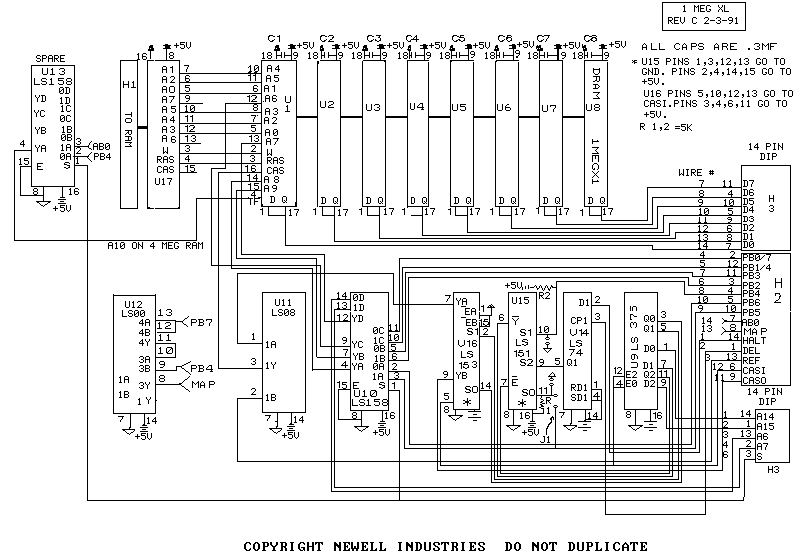
INSTALLATION INSTRUCTIONS FOR MEGXL REVISION C
This assumes that you have a Newell Meg Revision C board, or have made one to those specifications. This information is provided as is. It should be accurate, but I make no warranties that it is. Proceed at your own risk.
The MEG upgrade can be installed using different combinations of bits of the $D301 address port of the 6520 PIA. The 130XE uses bit 4 (low) to enable main CPU banking, and bit 5 to enable Antic banking. It uses bits 2 & 3 to determine which of the four 16K banks of memory is active. The 130XE uses 2 sets of ram banks and flip flops the CAS line to activate the banked memory. The Newell board uses the same method to bank into the added ram. After installation, your XL will be functionally compatible with an upgraded 130XE.
$D301 PORT B BIT ASSIGNMENTS FOR UNMODIFIED 130XE
BIT 0-OS ROM CONTROL, 1=ROM, 0=RAM
BIT 1-BASIC ROM CONTROL, 1=RAM, 0=ROM. NO CONNECT ON 1200XL
BIT 2-RAM BANK SELECT. NO CONNECT ON XL
BIT 3-RAM BANK SELECT. NO CONNECT ON XL
BIT 4-CPU BANKING ENABLE, 1=NOT, 0=ENABLED. NO CONNECT ON XL
BIT 5-ANTIC BANKING ENABLE, 1=NOT, 0=ENABLED. NO CONNECT ON XL
BIT 6-NOT USED
BIT 7-DIAGNOSTIC CONTROL, 1=RAM, 0=ROM
GENERAL INSTALLATION
The Newell board used a dip plug and ribbon cable for H2. The wire designations are 1(Red)=HALT, 2=DEL, 3=REF, 4=AB0, 5=AB1, 6=AB2, 7=AB3, 8=AB4, 9=AB5, 10=AB6, 11=CASO, 12=CASI, 13=MAP, 14=AB7. For H3, 1(Red)=A14, 2=A15, 3=A6, 4=A7, 5=SPARE, 6=S, & 7thru14=D7 to D0. If you are building your own board, you will have to determine how to get these connections from your board.
For 1200XL ONLY, do steps A-D. 800XL installations skip to 1.
Refer to drawing above:
A.Cut trace to pin 13 of U7. Cut traceto pin 11 of U10. Cut trace to pin 13 of U10.
NOTE:Make these changes on the bottom of the motherboard.
B.Install jumper wire from CPU address A7 to U10, pin 11. A7 was the trace that was going to U7, pin 3.
C.Install jumper wire from CPU address A13 to U7, pin 3. A13 is the trace that was going to U10, pin 13.
D.Install jumper wire from CPU address A14 to U10, pin 13. A14 is the trace that was going to U10, pin 11.
Test computer before continuing.
1.Remove the ram chip from U13(800XL), U6(1200XL). Install H1 cable in U13 or U6. Make sure the pins match up. Install the 64K ram chip in U17. Place the upgrade board on top of the ram, component side up.
2.On the PIA, remove pin 11(PB1) & 17(PB7) from the MB and bend them out.
3.Remove pin 8 of the 74LS51, U30(800XL), U25(1200XL). See drawings.
4.Connect the ribbon cable wires as follows:
Header H2
Wire to location            Wire to location
1    Antic IC pin 9         8    PIA IC pin 14
2    CO60472  pin 12        9         "     15
3    Antic IC pin 8         10        "     16
4    PIA pin      17        11   U30 hole   8(800XL), U25(1200XL)
5     "           11        12   U30 pin    8(800XL), U25(1200XL)
6     "           12        13   PIA hole   17 (1 meg ONLY)
7     "           13        14   PIA IC pin 10 (4 meg ONLY)
Header H3
Wire to location            Wire to location
1    Antic pin    19        8    Antic pin  31
2      "          20        9      "        32
3      "          26        10     "        33
4      "          25        11     "        40
5    No Connection          12     "        39
6 U29(800) U22(1200) 10     13     "        38
7    Antic pin    30        14     "        37
For 4 Meg installation, see Instructions to follow.
5.To be able to select internal Basic, connect a toggle switch betweeen ground and the hole for PIA pin 11(PB1).
6.Install 8 DRAM's (1 or 4 meg). 120ns min., CAS before RAS refresh.
7.Make sure there are no shorts and turn the computer on. If you did everything right, it should boot up as before. If not, fix it.
8.Assemble computer and retest.
$D301 PORT B BIT ASSIGNMENTS AFTER INSALLATION (1 MEG)

BIT 0-OS ROM CONTROL, 1=ROM, 0=RAM
BIT 1-RAM BANK SELECT.
BIT 2-RAM BANK SELECT.
BIT 3-RAM BANK SELECT.
BIT 4-CPU BANKING ENABLE, 1=NOT, 0=ENABLED. NO CONNECT ON XL
BIT 5-ANTIC BANKING ENABLE, 1=NOT, 0=ENABLED./ RAM BANK SELECT.
BIT 6-RAM BANK SELECT.
BIT 7-RAM BANK SELECT.
4 MEG INSTALLATION
Using 4 meg is NOT compatible with Basic XE, the translator disk, or any other software that requires bits 0 and/or 1 to remain in it's normal configuration. It does not allow Antic control, and the ram under the OS is lost.
1.Remove PIA pin 10 and bend up.
2. On the Newell Rev C board, cut traces J1 & J2 marked X, and strap to ground as indicated. Install a 74LS158 in U13.
3.Connect a toggle, or momentary switch between PB7 (PIA pin 17) and the hole. This switch is not required for the 1200XL unless you want to access the dianostics.
NOTE:This switch must be closed during power up (Atari & Omniview OS's) until you get a screen. It can be left off with the OSNXL OS. But it's required to enter Omnimon, Omniview, or the Atari diagnostics. It should be off at all other times.
All bits of $D301 are used for ram bank select.
Good luck.
Wes Newell
wnewell@ticnet.com
fidonet 1:124/7028
http://users.ticnet.com/newell
A note from AtariWorld Technicians: We are presently working on using a standard One meg SIMM with the above upgrade. Watch these pages for more information coming soon.
30 pin SIMM (30)
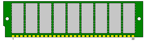
256k x 8, 256k x 9, 1 Meg x 8, 1 Meg x 9, 4 Meg x 8, 4 Meg
x 9
| Pin | Name | Description |
| 1 | Vcc | +5v DC |
| 2 | CAS | Column Address Strobe |
| 3 | DQ0 | Data 0 |
| 4 | A0 | Address 0 |
| 5 | A1 | Address 1 |
| 6 | DQ1 | Data 1 |
| 7 | A2 | Address 2 |
| 8 | A3 | Address 3 |
| 9 | GND | Ground |
| 10 | DQ2 | Data 2 |
| 11 | A4 | Address 4 |
| 12 | A5 | Address 5 |
| 13 | DQ3 | Data 3 |
| 14 | A6 | Address 6 |
| 15 | A7 | Address 7 |
| 16 | DQ4 | Data 4 |
| 17 | A8 | Address 8 |
| 18 | A9 | Address 9 |
| 19 | A10 | Address 10 |
| 20 | DQ5 | Data 5 |
| 21 | WF | Write Enable |
| 22 | GND | Ground |
| 23 | DQ6 | Data 6 |
| 24 | n/c | Not Connected |
| 25 | DQ7 | Data 7 |
| 26 | QP | Data Parity Out |
| 27 | RAS | Row Address Select |
| 28 | CASP | ? |
| 29 | DP | Data Parity In |
| 30 | VCC | +5V DC |
Note: QP, CASP, and DP are not connected on
non-parity (x8) SIMMs
A9 is not connected on 256k SIMMs
A10 is not
connected on 256k and 1 Meg SIMMs

