

 After building arid running the SmartOS in last year's issue, I decided that a few things were
not to my liking.
After building arid running the SmartOS in last year's issue, I decided that a few things were
not to my liking.
Out with the old
Top of the hit list were all those switches. I just don't like to drill a bunch of holes in my
1200XL case.... And, I keep leaving them in the wrong position. And, I can't remember which way is
up. And, it is an ordeal to load the RAM - lots of load this and change this switch and then load
that and change that switch and push this button. Out went the switches. Also, the programmable
internal cartridge just adds a lot of complexity with little benefit - out it goes, too. With these
changes, we can now load an OS image in a single, self-executing step. Memory writes can be
enabled or disabled from software and two complete SRAM OS versions (as well as the stock ROM OS)
are available electronically.
In With the New
Refer to the Smart IDE schematic. The switches have been replaced by an 8-bit latch (U5)
chat is selected at memory address $D180 by the HC138 decoder (U4). The bits in this latch are
all set to zero on powerup or RESET and control four functions: override, ROM select, write enable,
and RAM bank select. The default settings are therefore, no override (bit 7=0), SRAM select (bit
6=0), write disabled (bit 5=0). and SRAM bank 0 (bits 0-2=0). Lets discuss these functions one at
a time.
Bit Stuff
6
Bit 6: There are always those programs where any OS changes cause it to crash. Seems like some
people have to tweak just about everything they can... When this happens, the only recourse is to
use the stock OS and this is the function of bit 6. Although the default setting is for SRAM, you
can have the SRAM OS sec bit 6 at $D180 and JMP to RESET at $C2AA. This will put you into the ROM
OS on powerup and any time you hit the RESET key. To return to normal, just reload another SRAM OS.
7
Bit 7 (we took the bits a little out of order to make it easier to understand) Having no
switches is very nice for loading a new OS. Problem is - if you get an OS in there that will not
run, how do you load a new one? The default, powerup state is from the first SRAM bank. If that is
trashed, how do you fix it? Hmmmmmm.... No switches. OK, how about a joystick? Plug a joystick into
port 2 and hold down the fire button. This forces you into the ROM OS in the 1200XL, which will
always work. Store $40 into $D180 (bit 6, above) and you are latched into the ROM (let go of the
button). Works great! When you are using SRAM, just store $80 into $D180 (bit 7) and the joystick
fire button has no effect (so you can use the joystick normally). This is the function of the
override bit which should normally be set on somewhere in your SRAM OS code.
5
Bit 5 This is the write enable function that causes so much trouble in the switch version,
since having writing enabled while you are running seems to cause frequent data overlays. When bit
5 is zero (default), you cannot alter any of the SRAM data. Any routine that needs to write to SRAM
must first store $20 into $D180, which sets bit 5 on. It is good practice to set it back to zero
when you are done! This allows you to load an OS image from disk (or move it from ROM using
MOVEROM2.OBJ), enable SRAM writing with bit 5, and move the new image into one of your SRAM banks
(using MOVERAM2.OBJ) - all in one operation.
0-2
Bits 0-2 These bits select which 16K 0S segment you will be using in the $C000 to $FFFF
address range. Although the schematic shows a 32Kx8 SRAM, I used a 128Kx8 device in my latest unit.
So, instead of 2 05 banks, I now have 8 selections - all controlled by bits 0-2. (If you wire in a
128Kx8 SRAM, the A15 and A16 address bits from the chip go to bits 1 and 2 of the HC273 latch) If
you really want to get crazy and use a 5l2Kx8 SRAM, bits 3 and 4 are available.. (32 banks?)
Result
So, what did we end up with here? The SmartIDE is designed to allow you to run multiple
customized operating systems in your 1200XL and the address range at $D600 - $D7FF has been enabled
to provide usable space for new tables and software drivers. These features give you the ability to
easily modify the OS in your l200XL and the extra 512 bytes are a great place to run ramdisk
drivers, trace tables, mouse controllers, or keyboard function keys routines. (you may even see
some or all of these in future issues....)
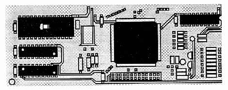
Building It
The construction of the original SmartOS used the OS ROM sites on the 1200XL to supply power
and signal lines. This IDE version uses the CPU socket instead, since the 6502 is more centrally
located and allows a much larger board to be used. The SmartiDE uses what I call a rip-off board
layout - one of the ICs on the motherboard is removed and it's socket is used to mount the new
board full of components (see figure 1). This provides two major benefits: wiring from the
motherboard to a daughterboard tends to be messy and fragile and it is easy to move your creation
to another l200XL if you have a reason to do so.
A Learning Experience
As an example, (now, pay attention - you wont want to learn this the hard way folks....) one
of my SmartIDE 1200XLs did not work after I plugged in a 65816 CPU.
OK, so maybe we have a problem with the Sweet 16 and my design. Nope, actually, I had
demonstrated this machine at an SLCC meeting and it did not run one of the DOM selections properly.
Since the IDE is fairly early in the development cycle, I assumed that it was a design problem in
the software. But, when I cried it the next day at home, it worked just fine. Hmmmmmmm. After
another problem appeared in an area that used to work, I decided it was not a design problem - the
l200XL was broken! I pulled out another 1200XL motherboard, modified it for the SmartIDE and tried
the board in that system. Now, everything works as it should - Sweetl6 and all. Very valuable
lessons. Make it easy to move a 'project' and thoroughly test anything before you modify it or
you'll take a trip down the garden path.
On Track Again
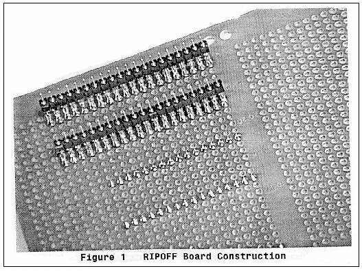
Back to the daughterboard. I used an old RadioShack project board chat I do not find in the
catalog. You can use the 276- 147 and trim off the excess. The terminal strips are the most
difficult part of any rip-off project. These are .5 inch long, .018 dia. double ended pins that
connect your board to the socket on the motherboard (see figure 1). They are not easy to find....
Do not use .025 square pins for this purpose - they are too large for the socket and will distort
the socket pins. If .025 is all you can find, replace the socket with something that will accept an
.025 pin properly. I found a supplier for Samtec part no. TS-132-G-AA pins some time ago and bought
what I thought was a lifetime supply. I guess I'm living longer than I thought because I'm running
low on pins. The Samtec company is still around (look on InterNet). Last phone number is
812+944-6733. Ask them for a distributor near you. If you really get stuck, I may have better
information after I try to get some more for my stock (a number of manufacturers make these kinds
of things - look around).
Easy Parts
The rest of the components are somewhat easier - IC sockets (put all your ICs in sockets), 40
pin DIP header, 10 pin DIP header, ICs and such. Mount them neatly on the daughterboard and wire
the circuit as shown in the schematic. Take a look at the upper left corner of the SmartIDE
schematic (at D8). The eight circles are the connector to the motherboard that connects us to chose
signals not available on the 6502. I used a 10 pin IDC connector and a flat cable soldered directly
to the motherboard. This still allows me to completely remove the daughterboard by disconnecting
the 10 and 40 pin connectors (at D8 and Cl). The six signals called out are:
| Dl | U18 pin 14 |
| D6 | U18 pin9 |
| D6 | U18 pin 7 |
| OS | right side of W12 (remove W12 jumper) |
| CSROM | left side of W12 |
| J/S | right side of R62 (below cart, port) |
As I said, these wires are soldered directly to a 10 conductor flat cable which plugs into the
10 pin header on the daughterboard.
 More Ripoff
Look closely at figure 1. The rip-off technique is to offset the new socket 0.1 inch from the
original position (which now holds the terminal strips soldered to the bottom of the daughterboard
and plugged into the original 6502 socket on thei motherboard). This gives us pairs of pins that
must be bridged with solder to reconnect the original signals. Carefully melt solder onto both pins
in each pair, using your iron tip as a link between the two pins. With a little practice, you will
be able to create a solder short between the two pins quite easily - much faster than using little
wires.... If you are not going to connect all the original circuit to the new 6502 location, do not
bridge that pair of pins, OK? (this project connects all the pins).
Soldering Tricks
When you are connecting more than one wire to a solder point, you may notice that the second
soldering operation melts all the solder on the pin and the first wire pops out of place. It takes
a little practice and a properly set iron temperature, but you can solder to just half of die pin.
Set your iron to the lowest temperature that will melt the solder. You need to do this so that the
whole pin will not melt at once. Solder the first wire on one side or die other of the pin. The
second wire will be soldered on the opposite side of the pin, holding the wire between the pin and
iron. This will heat the wire first, which will eventually begin to melt the solder on the pin
through the wire. This is not proper soldering procedure of course, but it does work well when you
only want to solder half of a pin After a second or so, die solder will begin to melt on die pin
and the wire will sink into the solder. Once this happens, remove the iron. You will find that only
about half of the solder on die pin has melted and the second wire is well connected, while the
first wire has not moved. Practice....
Getting Off th Ground
Once you have built the hardware, you inkeaninidalk~adinrothe SRAM. The circuit is designed so that
I bank 0 of the SRAM is enabled and write protected after poweron or RESET. At this point, SRAM is enabled and write protected after poweron or RESET. At this point, SRAM has no useful data in it - if you just power on your 1200XL, you will get a blank screen. Get out your joystick
and plug it into port 2. Or, make a small jumper and connect pins 6 and 8. Plug in your ED/ASM
cartridge, hold the trigger button down and power on the 1200XL. Still holding the trigger, go to
DEBUG and store a $40 into location $D180. Now, you can let go of the trigger. The system will stay
in the OS ROM unitl you zero bit 6 again at $D180.
ROM Image
If you have a ROM image of an operating system on disk, you can load it into memory at $4000
now. You cannot just load it into $0000 since you are a) in ROM at the moment and b) SRAM is write
protected. (you will be able to create a loadable unage if you follow die examples later in the
article) If you do not have an image on disk, move the stock OS in ROM into $4000 as a starting
point. To do this, load MOVEROM2.OBJ into memory from the ED/ASM editor. Go to BUG and 0600, which
runs the routine. Once finished, you can display $4000 and confirm that it now holds the same data
as $0000. Either way, you are now ready to load SRAM.
Into RAM
You can now load MOVERAM2.OBJ from die editor. Go to BUG and 0600 again. This will move the OS
from $4000 into the first bank of SRAM. From this point, you can power off or RESET - SRAM is
loaded in bank 0. The same procedure may be used to load die other SRAM banks, but you must alter
location $60E with the desired bank number before you run the routine.
Soft Where
Note:
MUOVEROU2 .ASM is unchanged from the version in the SmartOS article (MVROM.ASM) and will not
be listed again.
	0100 ; *** MOVERAM2.ASM  8/02/95	0430 LP2 JSR MOVEPAGE

	0110 ;     MOVES MEMORY INTO RAM	0440	CMP #$58

	0120 ;					0450	BNE LP2

	0130	*= $0600			0460 ;

	0140 ;					0470	LDA #$D8

	0150	PHP				0480	STA $CC

	0160	SEI				0490	BNE LP1

	0170	LDA $D40E			0500 ;

	0180	PHA				0510 MOVEPAGE LDA #$FD

	0190	LDA #$00			0520	STA $D301

	0200	STA $D40E			0530	LDA ($CD),Y

	0210 ;					0540	STX $D301

	0220 RAMON LDA #$A0			0550	STA ($CB),Y

	0230	ORA #$00			0560	INY

	0240	STA $D180			0570	BNE MOVEPAGE

	0250 ;					0580 ;

	0260	LDA #$00			0590	INC $CE

	0270	STA $CB				0600	INC $CC

	0280	STA $CD				0610	LDA $CC

	0290	LDA #$C0			0620	RTS

	0300	STA $CC				0630 ;

	0310	LDA #$40			0640 COMPLETE PLA

	0320	STA $CE				0650	STA $D40E

	0330	LDX #$70			0660	PLP

	0340	LDY #$00			0670	LDA #$FD

	0350 ;					0680	STA $D301

	0360 LP1 JSR MOVEPAGE			0690 ;

	0370 	BEQ COLPLETE			0700 RWOFF LDA #$C0

	0380	CMP #$D0			0710	STA $D180

	0390	BNE LP1				0720	BRK

	0400	LDA #$50			0730	.END

	0410	STA $CC

	0420 ;