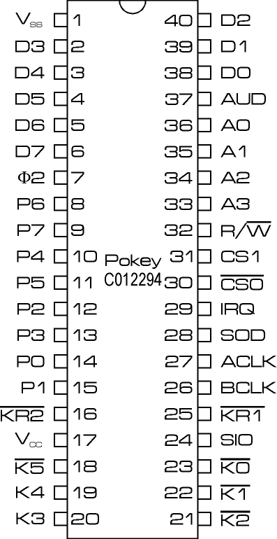

A vector graphic pinout is also available in Encapsulated PostScript format.
Note: I have no confirmation of the above descriptions. This is just my best educated guess, using my knowledge of microcomputer design, the function of the Pokey processor, and the interaction between the custom IC's.
 Back to Atari Technical Information page