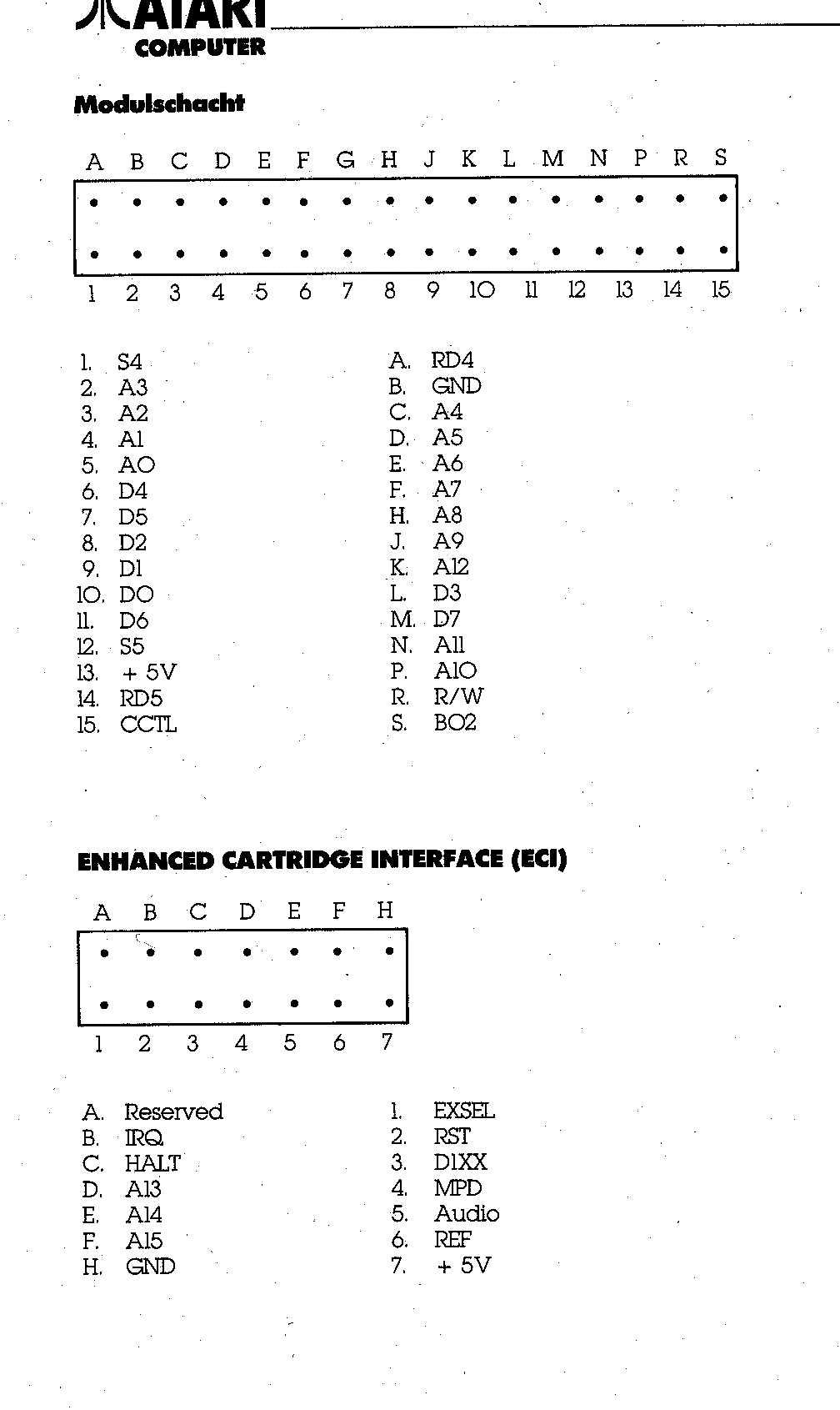
The
Atari XL Parallel Bus Interface - Part 2
By Roland
Scholz
Welcome to
part two of three in this series about the
parallel bus interface (PBI). Last time
we showed what signals the Atari 600/800XL
provides on the PCB edge connector at the
rear. If you own an Atari 800/130XE, the
signals have to be taken from the ROM module
plug and the ECI port, since Atari was too
stingy to provide the full plug as on the
previous generation.
 The question is how
we can use these signals to build a device
that is accepted by the Atari operating
system. The question is how
we can use these signals to build a device
that is accepted by the Atari operating
system.
Basically
Atari's engineers wanted a device that is
acknowledged by the computer in a plug-and-play
manner. In order to accomplish this during
the reset procedure, the bits of the register
at $D1FF (NEWPORT) are set to high level
in succession. The task of the PBI device
is now to map its own ROM at the position
of the Math ROM ($D800 - $DFFF). If the
Atari finds certain values (that are certainly
not contained in the Math ROM) at three
different addresses, the OS jumps through
a vector (also contained in the PBI ROM)
to an initialization routine for this device.
This routine is usually located in the PBI
ROM, too. What such a routine has to do
will be discussed in the next article. The
first thing to show here is how we can turn
off the Math ROM and turn on our own ROM
according to the settings of NEWPORT.
First of
all, we have to design a decoder that outputs
a logical "one" if the Atari writes
a certain value to NEWPORT. Such a decoder
is shown below.
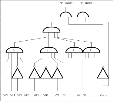
|
Figure 1: Decoder
for Newport ($D1FF) |
This
decoder outputs a high level at signal NEWPORTw
or NEWPORTr if a value is written to or
read from this address, respectively. The
next step is to save this value in a register
or flip-flop, because we need this signal
for more than just one clock cycle, since
the PBI has to be turned on, as long as
we do I/O through it.
TTL series
flip-flops of type 74xxx74 are suitable
for this. The "xxx" stands for
the type of TTL devices and tell you what
they are internally. I recommend the HCT
series, since they have quite low power
consumption, fast switching times and are
only little more expensive than ususal LS
devices.
For the TTLs
directly connected to the CPU bus, we have
to take care not to exceed the maximum fan-out
of one standard TTL at each PBI pin. One
standard TTL load is roughly equal to ten
HCT loads. Please now consider the circuit
shown in figure 2 that has the flip-flop
added. Input D1 of the flip-flop is connected
to one bit of the data bus. This could be
realized using an 8x2 plug and a jumper
that selects the bit you want to connect
to the flip-flop. This forms the address
of the PBI and since we can choose between
eight of them, there can be eight different
PBI devices connected the the Atari. The
clock input of the flip-flop is connected
through a NAND gate to the decoder taken
from figure 1 and the clock signal (Phi2)
of the Atari. As we know from the first
part of this series, the system clock PHI2
drives high level during the second half
of the cycle.
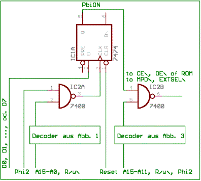
|
Figure 2: Circuit
for mapping PBI ROM to Math
ROM |
Since
the decoder also drives high level if there
happens an access to NEWPORT, we gain a
trailing edge at the output of the AND gate,
when the cycle ends. The flip-flop needs
a leading edge to store the bit at input
D, so we negate the signal, ending up with
a NAND gate. The flip-flop's RES input is
connected to the system reset signal, so
the device is definitely turned off during
power-on or after pressing the reset key.
We have a signal named PbiON that tells
us wether the device is on or off.
The next
task is to switch off the Math ROM and activate
our own ROM. To accomplish this, we have
to create a decoder that drives both singals
MPD\ (math-pack disable) and EXTSEL\ (external
select) to low level, if there is an access
to the storage area $D800 - $DFFF. In addition,
our ROM has to be selected using the ROM's
signals OE\ (output enable) and CS\ (chip
select). By the way, in the case signal
EXTSEL\ is not held low, the internal RAM
will be activated instead of the Math ROM,
so you can load your driver software there
without using a ROM. This should be done
for testing purposes only, since this is
not compatible with the PBI specification.
Figure 3
depicts such a decoder that is contained
in figure 2 as well. It decodes the addresses
between $D800 - $DFFF and only shows high
level during the second half of PHI2 and
if the CPU tries to read data.
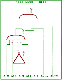
|
Figure 3: Decoder
for read access at $D800 - $DFFF |
This
signal is combined with PbiON throuh a NAND
gate again, so we get an active low output
if the device is turned on and there is
read access to the mentioned addresses.
With the described hardware one can build
a device that can map its own ROM into the
Atari if it is turned on. However, a "real"
device should also contain some sort of
I/O chips that perform, for instance, serial
or parallel I/O. Those chips will need a
special address area to access their configuration
registers and so on. Such addresses should
be mapped to the area just below NEWPORT,
like $D1F0 - $D1FE and only if the device
is activated. There are too many possibilities
to discuss the subject in depth.
However,
there is another thing interesting enough
to be mentioned: The PBI device can trigger
an IRQ interrupt! In order to do this, we
have to do the following:
First, the
interrupt signal of the PBI device must
be "wired-OR" to the IRQ signal
of the Atari. Having done this, we must
ensure the Atari reads a "1" at
NEWPORT from the bit assigned to the device.
Then the Atari will jump through a vector
in the PBI ROM. What we have to do on the
software side will be discussed in the next
article.
How can we
improve our circuit, so it enables the Atari
to read from NEWPORT? Please consider figure
4. Here again we use a flip-flop to store
the interrupt request. Through a tri-state
buffer (74126) the output of the flip-flop
is connected to the CPU data bus. Here we
use the same bit used to activate and address
our device. In general, tri-state chips
can assume in contrast to usual logic chips
three states, LOW, HIGH and ISOLATE, a third
state that puts the chip in high-impedance,
electrically disconnecting it from the surrounding
circuit.
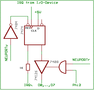
|
Figure 4: Circuit
for reading IRQ bit at NEWPORT
and assigning IRQ signal to
IRQ\ |
Once
again we need a decoder that tells us when
there is a read from NEWPORT. Please take
a look at figure 1 and you will notice the
output NEWPORTr that does exactly what we
want. Output D of the flip-flip connected
to IRQ in figure 4 should be of the open-collector
type, actually, but I've never had problems
just using a 1Kohm resistor. The signal
NEWPORTw is used to reset the flip-flop,
since we do not want the device to constantly
request interrupts. As the OS activates
the device using this line when an interrupt
request occurs, the request is surely deleted.
The last
thing to say is the aforementioned decoders
and logic can be easily built using GAL
(generic array logic) chips. These chips
contain logic elements (OR/AND gates, inverters)
that can be flexibly connected by programming
the chips. This programming is done electonically
and can be changed or adjusted nearly as
many times as you want. In order to show
clearly what the logic designs do, I have
used discrete gate symbols. The circuits
are not optimized or minimized, so they
are not recommended for practical use.
I hope this
article, in spite of its conciseness, has
been reasonably comprehensive and motivates
you to develop something useful for the
good old Atari. If there are questions or
suggestions please write to:
Roland Scholz,
roland_scholz@web.de
|
![[ Advert ]](images/banner.gif)